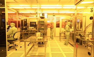
PN 生产线
PNDetector´s facilities comprise a full semiconductor fabrication line with 500 sqm clean room area of highest class specialized for the fabrication of double sided silicon radiation sensors with integrated electronics and 300 sqm for sensor packaging, qualification and system integration.
Moreover several workshops and development and application laboratories are available. Our talented teams are specialists in simulation and design, layout, semiconductor technology, electronics and mechanics. All our tools are state-of-the art.
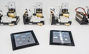
PNDetector´s focus is on advanced detectors for X-ray spectroscopy and imaging as well as electron detection and imaging. Detector types comprise p-i-n diodes in various designs for current measurement as well as diode arrays, Silicon Drift Detectors (SDDs) for spectroscopy and pixelated sensors like pnCCDs for imaging. All detectors are available as modules or systems.