The pnCCD (S)TEM Camera®
All pnCCD (S)TEM Camera® models provide the tremendous advantage of direct electron measurement. As no scintillator is required, the primary TEM electrons are absorbed directly in the sensor bulk and the created secondary charges are read out with highest precision. Hence ,PNDetectors’ pnCCD (S)TEM Camera® provides unique single electron detection sensitivity and simultaneously is capable to measure their energy with very high precision.
Key capabilities:
-
Unique single electron sensitivity SNR 300:1 (at 80 keV)
-
Ultra-fast readout:
-
2000 fps in full-frame mode (264 x264 pixel)
-
7500 fps using 4x binning (66x264 pixel)
-
Up to 10000 fps using windowing and binning (24 x264 pixel)
-
-
Wide energy range:
-
Standard range: 20 keV to 300 keV
-
Down to 5 keV possible
-
-
Two model options:
-
Fixed bottom camera (standard)
-
Retractable camera
-
-
Excellent radiation hardness
-
> 1x10¹⁸ TEM electrons (80 keV) per cm²
-
> 4x10¹⁷ TEM electrons (200 keV) per cm²
-

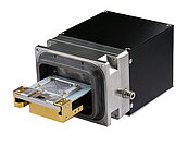
[Translate to Chinese:] Fixed bottom camera version
pnCCD System

pnCCD Properties
Fixed bottom camera

Retractable camera
PNOnline Software
Highlights
Working Principle
Electron Ptychography

Diffraction Pattern Analysis
Electric / Magnetic field mapping
Strain mapping

Single Electron Detection
Dynamic TEM Imaging
Low Voltage / Low Dose Imaging
(S)TEM Camera System Overview
Camera model options
- Fixed bottom camera
- Retractable camera
All (S)TEM camera models provide the following system components:
pnCCD Sensor
- Active sensor area of 12.7 mm x 12.7 mm
- Pixels: 264 x 264 full frame area, plus frame store
- Various readout modes:
- Imaging mode
- Anti-blooming mode
- Single electron mode
- High speed full frame operation
- Up to 1000 Hz
- Optional high speed mode: up to 2000 Hz
- Faster readout options with windowing and binning
- For details see pnCCD Properites
Complete electronics and data aquisition system
- Electronics mounted in 19 inch electronics rack and cPCI crate
- High speed parallel data acquisition
- Selectable amplification for high dynamic range
PNOnline Software
- Camera control
- Data acquisition
- Live visualization
- Live synthetic imaging
- Full raw data access

[Translate to Chinese:] pnCCD fixed bottom camera
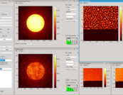
 bright field and dark field measured simultaneously in full frame mode (264x264 pixel) at 1 000 fps. (d-e) bright field intensity distribution measured in 4x binning mode (66x264 pixel) at 4 000 fps. Images (a,b) and (d,e) represent single frames, images (c) and (f) are averaged over 500 frames.")
[Translate to Chinese:] Example STEM measurements: (a-c) bright field and dark field measured simultaneously in full frame mode (264x264 pixel) at 1 000 fps. (d-e) bright field intensity distribution measured in 4x binning mode (66x264 pixel) at 4 000 fps. Images (a,b) and (d,e) represent single frames, images (c) and (f) are averaged over 500 frames.

The following camera specifications are valid for all pnCCD (S)TEM camera models.
| Physical pixel size | 48 µm × 48 µm × 450 µm |
|---|---|
| Number of physical pixels | 264 × 264 (69,696) full frame area, plus frame store area |
| Active area | 12.7 mm × 12.7 mm (161 mm2) full frame area |
| Frame rate in full frame mode | up to 1,000 fps (264 × 264 pixel) |
| Binning modes (examples) | 2-fold binning: 264 x 132 macropixel (2000 fps) 4-fold binning: 264 x 66 macropixel (4000 fps) |
| Windowing modes (examples) | 132 x 264 pixel (2000 fps) 24 × 264 pixels (10000 fps) |
| High speed Option | Up to 2000 fps in full frame mode (264 x 264 pixel) 4000 fps using 2-fold binning (264 x 132 macropixel) 7500 fps using 4-fold binning (264 × 66 macropixel) |
| Image integration time | down to 100 µs |
| Signal (per 80 keV primary electron) | 22000 signal electrons |
| Readout noise (RMS) | typically 30 signal electrons |
| Charge handling capacity | up to 400000 signal electrons per pixel |
| Radiation hardness | >1 x 10¹⁸ TEM electrons (80 keV) per cm² >4 x 10¹⁷ TEM electrons (200 keV) per cm² |
| Externally triggerable | Yes (accepts up to 4 triggers) |
Fixed bottom camera
The fixed bottom mount pnCCD (S)TEM Camera is designed to be easily mounted underneath the TEM – as a single device or in an additional camera housing below an already existing retractable third-party camera. It is also compatible to TEMs with an in-column filter (Omega filter). The camera head is equipped with a radiation hard lead shielding.
The fixed bottom pnCCD (S)TEM Camera enables the TEM to perform a wide range of experiments with excellent quality, please refer to the section Applications in STEM and Applications in TEM for examples. A selection of scientific publications from our pnCCD (S)TEM Camera® users is listed in the section Publications.
The synchronisation to an existing STEM unit can be realized custom specific.
This camera model is the preferred model option by our customers. Please contact PNDetector for more details on this camera, our technical staff will be happy to support you.

Retractable camera
The retractable pnCCD (S)TEM Camera® is designed to be bottom mounted underneath the fluorescent screen. The retractability offers the benefit of flexibility to use various camera systems without the necessity to unmount the camera from the TEM.
The synchronisation to an existing STEM unit can be realized custom specific.
Please contact PNDetector for more details on this camera and the mechanical constrains, our technical staff will be happy to support you.

PNOnline Software
The PNOnline software provides all the functionality necessary to control the PNDetector’s pnCCD (S)TEM camera system and conveniently acquire high quality data. Versatile live displays provide instantaneous feedback about the bright field disk or diffraction pattern on the detector and allow effective adjustment of the camera settings. Data can be recorded in STEM or TEM measurement mode and is saved in PNDetectors’ frms6 file format which guarantees full raw data access, and can easily be used with common data analysis frameworks, like the LiberTEM project. Various masks can be selected for flexible live synthetic imaging.
Key features:
-
Control of camera system
-
Camera modes
-
Readout modes
-
Gain
-
-
Versatile live displays
-
Single frame
-
Average frame
-
Running average
-
Synthetic image
-
Centroid X/Y
-
-
Recording data
-
STEM / TEM mode
-
Full raw data access (.frms6 data format)
-
-
Synthetic imaging
-
Live synthetic imaging with various mask shapes
-
-
Documentation
-
Text file with meta data
-
Electronic logbook
-

The pnCCD (S)TEM Camera® is a pixelated, fast, radiation hard, and direct electron imager for applications in both TEM and STEM
Due to its outstanding signal to noise ratio of 300:1 (for 80 keV electrons), single primary electron measurement from 20 keV to 300 keV is possible. With its high readout speed of up to 7500 frames per second (133 µs dwell time) the pnCCD camera opens up new scientific and analytical possibilities in electron microscopy such as 4D-STEM imaging and low dose / high speed TEM imaging.
NEW scientific techniques
With the unique properties of the pnCCD (S)TEM Camera® new scientific techniques become accessible.
In STEM, the full 2D scattering pattern can be recorded for each probe position at high speed and high granularity providing 4D datasets of the sample. This enables sophisticated techniques like Ptychography where the amplitude and phase information can be completely recovered and used to produce high quality images of weakly scattering material. The 4D datasets further allow to precisely determine the position bright field disks or diffraction reflexes enabling the measurement of electrical and magnetic fields as well as strain.
In TEM, single electron measurements are possible with energies down to 20 keV. Highly dynamic processes can be observed with a time resolution well below 1 ms.

NEW post processing and post correction possibilities for STEM
The pnCCD (S)TEM Camera® provides full access to the raw data. This enables highly flexible post processing schemes. For example, synthetic images can be calculated by applying virtual apertures on a 4D dataset. By using this virtual diffraction imaging the user can extract BF, ABF, DF, ADF, HAADF and many more synthetic images. With ptychographic analysis it is possible to change the focus and even correct aberrations after the measurement.
NEW efficient workflow
Due to its extreme radiation hardness the pnCCD® can be used for both alignment and recording allowing the operator an efficient workflow. The high performance software PNOnline calculates synthetic images real time by applying user-selectable, virtual apertures to the recorded data while recording a measurement. The camera can be fine-tuned to the operators’ experimental needs by using dedicated operation modes: The single electron mode allows for the best resolution in low dose conditions. The imaging mode is ideal for quantitative analysis and the anti-blooming mode suppresses charge spilling.

The pnCCD® Principle
The pnCCDs are back illuminated, three-phase CCDs on a fully depleted silicon substrate. Their operation is based on the principle of sideward depletion and on transfer registers formed by pn-junctions. The outstanding characteristics include a homogeneous and thin photon entrance window leading to high quantum efficiency values between 100 eV and 20 keV and an excellent radiation hardness as well as high charge handling capacity.
Electron ptychography
Electron ptychography is a 4D-STEM technique that was described theoretically in 1993 but so far was limited experimentally by the low readout speed of existing cameras. In this technique, the intensity distribution in the bright field disk is recorded in 2D for each STEM probe position. In an electron waveoptical approach, the phase and amplitude information is extracted from the recorded intensity images. The reconstructed phase image shows enhanced image contrast compared to the conventional annular dark field image.

Diffraction Pattern Analysis
Information like crystal structure and phases, lattice defects, or strain along interfaces can be determined by 2D diffraction pattern analysis. Recording the 2D diffraction pattern for each probe position with the pnCCD (S)TEM Camera® allows any pattern region or diffraction peak to be analysed from the raw data without loosing the conventional, well-established STEM view. The example of a measurement of a meteorite sample shown on the right side demonstrates the scientific benefit of this capability. A selective area diffraction (SAD) analysis was done by selecting single diffraction discs to generate multiple synthetic STEM images.

Electric / Magnetic field mapping
With the pnCCD (S)TEM Camera®, small shifts of the bright field disc (BFD) can be detected providing information about magnitude and direction of local electric fields, magnetic fields or mechanical disturbances.
-
The pnCCD® gives the full intensity information of the BFD with 264x264 pixels for each STEM pixel position.
-
Information rich raw data is stored and provides the flexibility to apply various disk finding algorithms.
-
Thus, a precise determination of disk positions even in difficult situations such as a blurred or cropped BFD, is possible.
 Centroid image in y-direction at 0 V and
(b) at 50 V.
(c) difference of (a) and (b).
(d) Vector field proportional to the local electric field calculated from shifts of the BFD position in x- and y-direction. Additionally, the background color emphasizes the field direction. The inset shows a STEM image simultaneously acquired with an ADF detector. In collaboration with FZ Jülich")
[Translate to Chinese:] Electric field around a tungsten needle. Shifts of the BFDs are calculated from 4D-STEM datasets acquired with and without applied voltage. (a) Centroid image in y-direction at 0 V and (b) at 50 V. (c) difference of (a) and (b). (d) Vector field proportional to the local electric field calculated from shifts of the BFD position in x- and y-direction. Additionally, the background color emphasizes the field direction. The inset shows a STEM image simultaneously acquired with an ADF detector. In collaboration with FZ Jülich
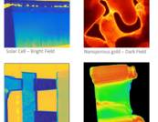
Strain mapping
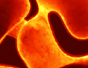
The measurements of lattice strain is a highly valuable technique to investigate sample quality and to depict lattice strain induced e.g. due to the sample growth process and/or material combination. The pnCCD camera provides high quality measurement results at high readout speed.
The image depicts a measurement of a nanoporous gold sample. The left figure shows a running average (1000 frames) image recorded in the anti-blooming mode. The full image (right figure) of 256 x256 STEM sample points was recorded with 1000 fps and therefore was acquired in only 4.5 minutes.
 Running average image (1000 frames) of a nanoporous gold sample recorded in anti-blooming (AB) mode.
(b) STEM dark field image of the nanoporous gold sample: 4 frames where acquired for each of the 256 x256 STEM sample points at 1000 fps.
In cooperation with University of Bremen")
[Translate to Chinese:] (a) Running average image (1000 frames) of a nanoporous gold sample recorded in anti-blooming (AB) mode. (b) STEM dark field image of the nanoporous gold sample: 4 frames where acquired for each of the 256 x256 STEM sample points at 1000 fps. In cooperation with University of Bremen
Single Electron Detection
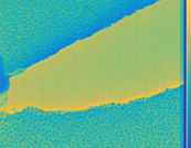
Due to its extremely high signal-to-noise ratio of 300:1 at 80 keV, the pnCCD (S)TEM Camera® provides the capability of single electron measurement. Examples of measurements which demonstrate the benefit of this capability are shown on the right side. Each pattern in image (a) shows the signal of a single primary electron (80 keV).
Depending on the experimental requirements, some of our customers are interested in a spatial resolution beyond the pnCCD pixel size of 48 µm. A method to archive the so-called “computational sub-pixel resolution” is based on dedicated data post-processing and was described (for X-ray applications) by S. Ihle et al. (2017), please refer to this publication for a detailed discussion. Single electron events can also be processed to receive images with a spatial resolution better than the physical pixel size. This method is based on advanced center of gravity algorithms. It factors in the track and the distribution of the signal electrons in the detector that have been created by the primary electron. As the frms6 data format provides the full raw data information, it enables the user to develop this post-processing step and to apply it “on demand” on any pnCCD (S)TEM Camera® data recorded in the frms6 format which meets the requirements for successful subpixel-analysis, e.g. regarding the count rate.
Figure (b) shows an example for an electron hologram before (top) and after subpixel processing (bottom). Comparing the line proles (red and blue curves in the graph on the right side) demonstrates the improved resolution of the interference pattern.

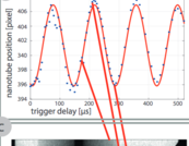
Dynamic TEM Imaging
Based on the high readout speed of 1000 fps in full frame mode and up to 8000 fps with windowing and binning mode, the pnCCD (S)TEM Camera® gives the possibility to investigate chemical or physical processes in the 0.1 - 1 ms regime. This capability is demonstrated by the experiment shown on the right side, where the induced resonant oscillation of a freestanding CdS nanowire was measured. The readout of the camera was externally triggered with a variable delay with respect to the zero crossing of the sine function driving the oscillation with 1.85 kHz. The analysis of the position of the nanowire acquired by this measurement revealed the resonant frequency of the nanowire to be approximately 4 times the excitation frequency. Elastic properties of the nanowire can be deduced from these measurements through further analysis.

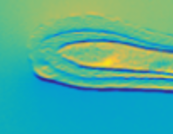
Low Voltage / Low Dose Imaging
The exceptional high sensitivity allows precise measurement of low energy electrons, down to 5keV. Shown here is a TEM image acquired at 30keV and 1000 fps. The image shows the average of 30 frames. The PNOnline software provides the capability to calculate and display such running average images at TV speed (30Hz).
